Quality control (2)/Semiconductor Engineering 15

Semiconductor - pn junction Current / Ideal I-V relationship - Assumption

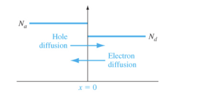
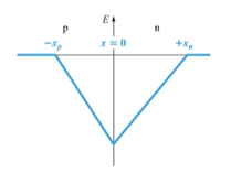
Ideal I-V relationship - Assumption Assumption ideal한 pn junction을 만들기 위하여 다음과 같은 가정이 필요하다. 1. The abrupt depletion layer approximation applied. The space charge regions have abrupt boundaries, and the semiconductor is neutral outside of the depletion region. ( Space charge region은 급격한 경계를 가지며, semiconductor는 원하는 위치에만 정확하게 도핑된다. Semiconductor는 Space charge region 영역 밖에서는 중립적이다.) 위 그림에서 확인할 수 있듯이..

Semiconductor - Ch7-1(4) / Zero Applied Bias / Electric Potential / Space Charge Width

Electric Potential Electric Potential과 Electric Field의 관계 전자기학에서 가장 기본적으로 다루었던 이야기이다. (Ch4,Ch6) E-field를 적분한 것의 음수가 Electric Potnetial이 된다. E-field를 통해 E-Potential 계산 [In the P region] 적분을 하면 적분 상수가 생기므로 Boundary Condition을 통해 적분상수를 계산해야 E-potential 식이 완성된다. Boundary Condition을 대입해서 계산하면 적분상수가 아래와 같이 나온다. p region에서의 Electric Potential의 식은 다음과 같다. 그래프로 나타내었을 때 그 기울기는 제곱으로 증가하고 있다. (아래에서 다시 설명 ) ..

Semiconductor - Ch7-1(3) / Zero Applied Bias / Electric Field

Electric Field 생성 Electric Field 생성 - [내부 charge separation에 의한 E-filed 생성] junction이후 diffusion이 일어나고 negative charge density와 positive charge density의 분리에 의해 depletion region 즉,Space charge region에 생성되며 E-field가 생성된다. (E-filed is created in the depletion region by the separation of positive and negative space charge densities.) - [ 거리에 따른 부피 전하 밀도(charge density) ] pn junction에 따라 p type과 n ty..

Semiconductor - Ch7-1(2) / Zero Apllied Bias / Built-in potentail (barrier)

Zero Applied Bias Introduction (Zero Applied Bias) - 전류가 존재하지 않고, 외부 자극도 없는 열적 평형 상태에서의 pn junction의 특징 ( The properties of the pn junction in thermal equilibirium, where no currents exist, and no external excitation is applied.) [ Zero Applied Bias에서 다루게 될 것 ] - (1) built-in potential barrier - (2) E-field and potential through the depletion region - (3) space charge region width (=W) Zero Appl..

Semiconductor - Ch7-1(1) / PN junction / diffusion / Space charge region / E-field Force /

Basic Structure of the pn junction Introduction We will consider the situation in whcih p-type and n-type semiconductor are brought into contact with one another to form a pn junction. (p-type 반도체와 n-type이 결합된 것을 pn junction이라 부른다.) // Metallurigical Junction (금속적 결합) The electrostataics of the zero-biased and reverse-biased pn junction will be considered. (thermal equilibrium상태에서 두 가지 case) - z..

Semiconductor - Fabrication example / pn junction

PN Junction Fabrication Example ( PN-junction ) : 간단히 , p형 반도체와 n형 반도체가 접합되어 서로 상호작용하는 구조를 말한다. What is PN-junction : p형 반도체는 양전하를 가진 고농도의 활성원자를 포함하고 있고, n형 반도체는 음전하를 가진 고농도의 활성원자를 포함하고 있다. 이러한 p형 실리콘과 n형 실리콘을 접합시키면, n형 실리콘에서 p형 실리콘으로 이동하는 전자와 p형 실리콘에서 n형 실리콘으로 이동하는 정공이 만낙 된다. 전자와 정공이 만나면 서로 상쇄되어 사라지며, 이 과정에서 발생하는 에너지는 빛으로 방출된다. 이것이 pn 접합 다이오드에서 빛이 나오는 이유이다. 다이오드, 트랜지스터, LED를 만드는 데 필수적인 구조이다. pn..

Semiconductor- Ch3-2 / Energy gap / (in)direct / Density of State(DOS) / Statical Mechanics

Energy gap Insulator Semiconductor Metal( Conductor) Energy Gap 3.5~3.6eV 이거나 그 이상인 것 대략 1eV인 것 Si semiconductor은 300K에서 v alance band's electron이 conduction band로 올라간다. 0에 가깝거나 0보다 작아서 overlap 낮은 에너지에서도 전류가 쉽게 흐름 Energy gap의 특성에 따라 electrical conductivity를 정의할 수 있다. Conductivity : 전류가 얼마나 잘 흐르게 하느냐 Resistivity : 전류가 얼마나 잘 흐르지 못하게 하느냐 (저항) Direct & Indirct Energy gap Direct bandgap : 3족. 5족 원소들 ..

Semiconductor - Ch2-2 / Schrodinger's Wave equation

Schrodinger's Wave Equation Schorodinger's Wave Equation - 거리에 따른 전기장과 시간에 따른 전기장은 속도로 연관되어 있다. 이를 슈레딩거에 적용하여 원자의 위치, 시간 등을 예측해보고자 한다. - 슈레딩거 wave equation은 quantum mechanics의 중요한 개념 중 하나로, 시간에 따른 양자 시스템의 움직임을 예측하는 수학적 방정식이다. - 슈레딩거 wave equation은 입자의 위치(x) 운동량(p)에 대한 정보를 제공한다. 이 방정식은 양자의 상호작용과 에너지 양자화를 설명하는 데에 사용한다. - 이 방정식은 wave-particle principle의 기초가 되며, 일반적으로 허수 방정식으로 표현된다. - 양자역학에서 입자의 위칭나..

Semiconductor - Ch2-1 / Quantum Mechanics/ photoelectric effects(Energy Quanta, Wave duarlity, Uncertainty )

Quantum Mechanics Electron & Hole : 크기가 작고 질량도 작아서 우리가 알고 있는 일반 물리학 적용이 안 된다. (결과가 불확실) 전자와 정공에 대해서는 Quantum(양자) Mechanics(역학) 도입이 필요하다. //확률적 접근 ** 양자 : 에너지가 연속적이지 않고, 뚝뚝 끊어져있다. or 수치화 되어있다. 연속적이지 않은! (이산화 된 에너지) ** 역학 : 물체의 운동 거시적인 움직임 vs cubic 안에 전자가 있을 확률 Semiconductor Energy gap (C) Semiconductor : 외부의 에너지(빛. 열, 전압 etc..)에 의해서 전류가 흐를 수 있게 만들 수 있는 것으로, 외부 에너지에 의해 valence band에 있는 전자가 conduct..

Semiconductor - Ch1-2 / Crystal plane & direction / Diamond Structure / Imperfections & impurities

Space Lattices ( Crystal plane & Direction ) hole & electron : 힘의 단위로 보통 N(뉴턴)을 쓰나, hole과 electron은 너무 작아서 F=ma와 같은 물리법칙을 따르지 않는다. 따라서 전자와 정공에 대해서는 확률을 기반으로 한다. Crystal Planes ( 면 ) - Semiconductor device는 surface에서 fabricated된다. 그래서 surface는 semiconductor device의 특징을 결정짓는 중요한 요소가 된다. - We can describe these surfaces in terms of the lattice //격자로 표면을 표현할 수 있다. - Miller indices : crystal plane ( ..