분류 전체보기 232

[ DX 부문 ] 영상 디스플레이 사업부(VD) / 회로개발 직무 분석

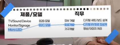
영상디스플레이 사업부 회로개발 youtube.com/watch?v=WdZosdW8k9U&list=PLTHa7qutpLjCrQEHA5KXDnT7MwKlb2jcK&index=12 VD 사업부 (영상 디스플레이 사업부) : 다양한 환경에 맞는 최적의 display 제품을 개발해 소비자에게 최고의 솔루션을 제공하고 소비자 개개인의 라이프스타일을 반영한 제품을 개발하는 부서 이광호 프로 : VD사업부의 혁신제품개발 Lab 제품선행 FPGA 파트 근무 제품마다 있는 analog 회로 위에 Firmware를 얹어서 실제 전기적 신호를 컨트롤 하고 불이 들어오게끔 연구(TV나오도록) 혁신 제품 개발 Lab : LED 기반의 디지털 사이니지와 Micro LED 디스플레이 "The wall" 제품의 TCON,FPGA(fi..

[삼성 반도체] 회로설계 엔지니어 직무분석

Samsung (team. DT) team.DT : 플랫폼 레벨의 제품 특성을 확보하기 위하여 설계 관련된 솔루션을 제공하고 설계 방법론을 제공하는 그룹이다. 다양한 부품을 어떤 순서에 맞게 어떻게 배치하냐. 부품 배치도나 설계도 등 어떻게 조립하느냐에 대한 설계를 진행한다. 이러한 디자인 가이드를 DM(Design Methodlogy, 디자인 방법론)이라 한다. SI(Signal Integrity , 신호 품질 측정) : 이는 SOC 칩에서 메모리칩으로의 양방향 통신에서 어떻게 하면 보다 신호전달이 잘 되고, 적은 파워 소모로 동작이 가능한지를 따져보고, 어떠한 구성환경을 갖추어야 되는지 시뮬레이션을 통해서 검증하고 실제로 칩이 나왔을 때, 동일한 환경에서 측정해서 DM solution이 정확한지에 대..

Semiconductor - pn junction Current / Ideal I-V relationship - Assumption

Ideal I-V relationship - Assumption Assumption ideal한 pn junction을 만들기 위하여 다음과 같은 가정이 필요하다. 1. The abrupt depletion layer approximation applied. The space charge regions have abrupt boundaries, and the semiconductor is neutral outside of the depletion region. ( Space charge region은 급격한 경계를 가지며, semiconductor는 원하는 위치에만 정확하게 도핑된다. Semiconductor는 Space charge region 영역 밖에서는 중립적이다.) 위 그림에서 확인할 수 있듯이..

Verilog - LFSR( Linear feedback shift register ) / Fibonacci & Galois LFSR

LFSR LFSR이란? : Linear Feedback Shift Register의 약자로, 선형 되먹임 시프트 레지스터이다. Shift Register에 입력되는 값이 이전 상태의 선형 함수로 다시 되먹임되는 Linear Feedback구조이다. 이전 상태가 Feedback되어 다음 상태를 만들기 때문에 "결정론적이다"라고 할 수도 있다. Fibonacci LFSR module fibonacci_LFSR( input clk, input arst_n, output LFSR ); parameter BITWIDTH = 5; //bitwidth만큼 reg생성 output reg [BITWIDTH -1 : 0 ] LFSR; always @(posedge clk or negedge arst_n) begin if(..

Semiconductor - Ch7-1(4) / Zero Applied Bias / Electric Potential / Space Charge Width

Electric Potential Electric Potential과 Electric Field의 관계 전자기학에서 가장 기본적으로 다루었던 이야기이다. (Ch4,Ch6) E-field를 적분한 것의 음수가 Electric Potnetial이 된다. E-field를 통해 E-Potential 계산 [In the P region] 적분을 하면 적분 상수가 생기므로 Boundary Condition을 통해 적분상수를 계산해야 E-potential 식이 완성된다. Boundary Condition을 대입해서 계산하면 적분상수가 아래와 같이 나온다. p region에서의 Electric Potential의 식은 다음과 같다. 그래프로 나타내었을 때 그 기울기는 제곱으로 증가하고 있다. (아래에서 다시 설명 ) ..

Verilog - Finite State Machine (FSM) / Lemming Game

FSM(Moore)을 이용한 Lemming Game(1) [Problem] Design source code //RTL code module Lemmings1( input clk, input rst_n, input bump_left, input bump_right, output walk_left, output walk_right ); //explicit expression localparam LEFT = 0, RIGHT = 1; reg present_state, next_state; //next_state compuation always @(*) begin //next state computation logic - Combinational Logic case (present_state) LEFT : ne..

Semiconductor - Ch7-1(3) / Zero Applied Bias / Electric Field

Electric Field 생성 Electric Field 생성 - [내부 charge separation에 의한 E-filed 생성] junction이후 diffusion이 일어나고 negative charge density와 positive charge density의 분리에 의해 depletion region 즉,Space charge region에 생성되며 E-field가 생성된다. (E-filed is created in the depletion region by the separation of positive and negative space charge densities.) - [ 거리에 따른 부피 전하 밀도(charge density) ] pn junction에 따라 p type과 n ty..

Semiconductor - Ch7-1(2) / Zero Apllied Bias / Built-in potentail (barrier)

Zero Applied Bias Introduction (Zero Applied Bias) - 전류가 존재하지 않고, 외부 자극도 없는 열적 평형 상태에서의 pn junction의 특징 ( The properties of the pn junction in thermal equilibirium, where no currents exist, and no external excitation is applied.) [ Zero Applied Bias에서 다루게 될 것 ] - (1) built-in potential barrier - (2) E-field and potential through the depletion region - (3) space charge region width (=W) Zero Appl..

Semiconductor - Ch7-1(1) / PN junction / diffusion / Space charge region / E-field Force /

Basic Structure of the pn junction Introduction We will consider the situation in whcih p-type and n-type semiconductor are brought into contact with one another to form a pn junction. (p-type 반도체와 n-type이 결합된 것을 pn junction이라 부른다.) // Metallurigical Junction (금속적 결합) The electrostataics of the zero-biased and reverse-biased pn junction will be considered. (thermal equilibrium상태에서 두 가지 case) - z..

Semiconductor - Fabrication example / pn junction

PN Junction Fabrication Example ( PN-junction ) : 간단히 , p형 반도체와 n형 반도체가 접합되어 서로 상호작용하는 구조를 말한다. What is PN-junction : p형 반도체는 양전하를 가진 고농도의 활성원자를 포함하고 있고, n형 반도체는 음전하를 가진 고농도의 활성원자를 포함하고 있다. 이러한 p형 실리콘과 n형 실리콘을 접합시키면, n형 실리콘에서 p형 실리콘으로 이동하는 전자와 p형 실리콘에서 n형 실리콘으로 이동하는 정공이 만낙 된다. 전자와 정공이 만나면 서로 상쇄되어 사라지며, 이 과정에서 발생하는 에너지는 빛으로 방출된다. 이것이 pn 접합 다이오드에서 빛이 나오는 이유이다. 다이오드, 트랜지스터, LED를 만드는 데 필수적인 구조이다. pn..